Advantages of High Density Interconnect
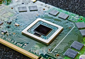
High Density Interconnect PCBs are ideal for modern digital devices that require smaller form factors and increased functionality. The HDI process prioritizes miniaturization and features multiple layers of tightly stacked circuitry with microvias, fine-pitch components, and advanced surface finishes like ENIG. This specialized manufacturing process results in a PCB that is more cost-effective and efficient than traditional options.
The main advantage of high density interconnect is its ability to accommodate more components in a small space. This translates to reduced overall device size, weight, and power consumption. In addition, the shorter distance between components leads to faster signal transmission times and lower risk of loss or interference.
This type of PCB is ideal for a wide variety of electronic devices, including portable computers, mobile phones, MP3 players, and video game consoles. It is also commonly used in medical equipment, such as monitors, surgical tools, and diagnostic systems. In addition, many IoT (Internet of Things) devices use high density interconnect technology to communicate with other electronic components and relay usage information to a cloud-based system.
Advantages of High Density Interconnect PCBs
While HDI PCBs offer numerous advantages, they can be challenging to design properly. It is important to pay attention to the number of sequential laminations and the type of via structure used, as these can have a significant impact on circuit performance. Additionally, it is critical to avoid unnecessary Staggered Vias and Extra-Large Inner Connects (ELIC) whenever possible. These features reduce routing efficiency and increase the amount of solder mask clearance needed, which can impact tracing widths and pad sizes in 1 mm pitch BGAs.
When designing an HDI PCB, it is essential to keep in mind the manufacturing constraints and capabilities of the manufacturer. This will ensure that the board can be produced effectively and to your specifications. It is also crucial to consider the thermal properties of your material choice, as well as its ability to withstand the required soldering temperatures.
Finally, it is important to review the manufacturing tolerances and design rules of your manufacturer before choosing a stackup for your PCB. This will help you avoid any issues that may arise during production, such as mismatched pads or traces.
The high-density interconnect PCB process involves several steps, including a careful selection of materials, laser drilling of microvias, layer lamination with insulating material, copper plating and etching for precise circuit patterns, application of advanced surface finishes like ENIG, and the assembly of fine-pitch components and high-density interconnects. These steps, combined with rigorous quality control and testing, produce high-quality boards that are suitable for a wide range of applications. For example, automobile manufacturers use these PCBs to incorporate advanced electronics in their vehicles, resulting in more compact devices that provide enhanced safety and functionality. Moreover, these devices can be assembled with fewer raw materials than conventional PCBs. Hence, they are more cost-effective and environmentally friendly than other options. Consequently, these advanced PCBs are becoming increasingly popular in the industry. In the future, it is likely that all digital devices will be constructed using this cutting-edge technology.